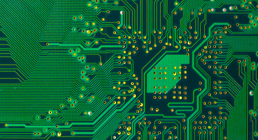
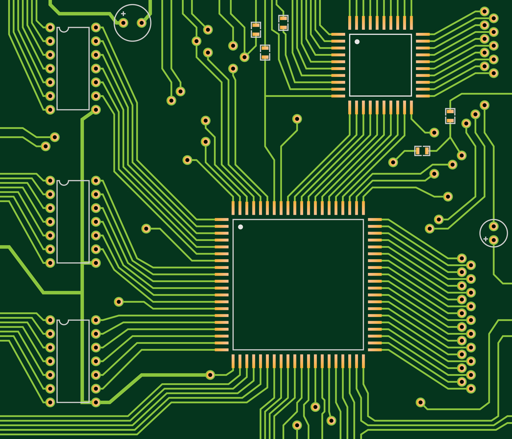
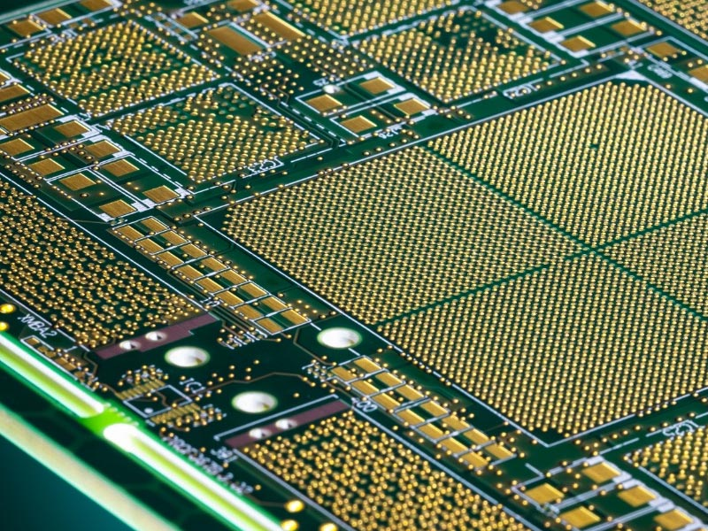
Printed circuit boards are necessary components of most electrical devices. Today’s PCBs have several layers to them: the substrate, traces, solder mask, and silkscreen. One of the most important materials on a PCB is copper, and there are several reasons why copper is used instead of other alloys like aluminum or tin.
What are PCBs Made Of?
Stated by a PCB assembly company, PCBs are made of a substance called a substrate, which is made of fiberglass that is reinforced with epoxy resin. Above the substrate is a layer of copper foil that can be bonded on both sides or only one. Once the substrate is made, manufacturers place the components on it. They use a solder mask and silkscreen along with resistors, capacitors, transistors, diodes, circuit chips, and other highly specialized components.
Why is Copper Foil Used in PCBs?
PCB manufacturers use copper because it has superior electrical and thermal conductivity. As the electrical current moves along with the PCB, the copper keeps the heat from damaging and stressing the rest of the PCB. With other alloys – like aluminum or tin – the PCB could heat unevenly and not function properly.
Copper is the preferred alloy because it can send the electrical signals across the board without any problems losing or slowing down the electricity. The efficiency of the heat transfer allows manufacturers to install classic heat sinks on the surface. Copper itself is efficient, as an ounce of copper can cover a square foot of PCB substrate at 1.4 thousandths of an inch or 35 micrometers thick.
Copper is highly conductive because it has a free electron that can travel from one atom to the other without slowing. Because it remains just as efficient at that incredibly thin level as it does at thicker levels, a little copper goes a long way.
Copper and Other Precious Metals Used in PCBs
Most people recognize PCBs as being green. But, they usually have three colors on the outer layer: gold, silver, and red. They also have pure copper inside and outside of the PCB. The other metals on the circuit board show up in various colors. The gold layer is the most expensive, the silver layer has the second-highest cost, and the red is the least expensive layer.
Using Immersion Gold in PCBs
copper on printed circuit board
The gold-plated layer is used for connector shrapnel and component pads. The immersion gold layer exists to prevent the displacement of surface atoms. The layer is not just gold in color, but it is made of actual gold. The gold is incredibly thin but is enough to extend the lifespan of the components that need to be soldered. The gold prevents the solder parts from corroding over time.
Using Immersion Silver in PCBs
Silver is another metal used in PCB manufacturing. It is significantly less expensive than gold immersion. Silver immersion can be used in place of gold immersion because it also helps with connectivity, and it reduces the overall cost of the board. Silver immersion is often used in PCBs that are used in automobiles and computer peripherals.
Copper Clad Laminate in PCBs
Instead of using an immersion, copper is used in a clad form. This is the red layer of the PCB, and it is the most commonly used metal. The PCB is made from copper as the base metal, and it is necessary to get the circuits to connect and speak to each other effectively.
How is Copper Foil Used in PCBs?
Copper has several uses in PCBs, from the copper-clad laminate to the traces. Copper is vital for PCBs to work appropriately.
What is PCB Trace?
A PCB trace is what it sounds like, a path for the circuit to follow. The trace includes the network of copper, wiring, and insulation, as well as the fuses and the components that are used on the board.
The easiest way to understand a trace is to think of it as a road or bridge. To accommodate vehicles, the trace needs to be wide enough to hold at least two of them. It needs to be thick enough not to collapse under pressure. They also need to be made of materials that will withstand the weight of the vehicles that travel on it. But, traces do all of this to a much smaller degree to move electricity rather than automobiles.
Components of PCB Trace
There are several components that make up the PCB trace. They have various jobs that need to be done for the board to do its job adequately. Copper has to be used to help the traces do their jobs, and without the PCB, we would not have any electrical devices. Imagine a world without smartphones, laptops, coffee makers, and automobiles. That is what we would have if PCBs did not use copper.
PCB Trace Thickness
The PCB design depends on the thickness of the board. The thickness will affect the balance and will keep the components connected.
PCB Trace Width
The width of the trace is also important. This does not affect the balance or the attachment of the components, but it does keep the current transferring without overheating or damaging the board.
PCB Trace Current
The PCB trace current is necessary because this is what the board uses to move electricity through the components and wires. Copper helps this happen, and the free electron on each atom gets the current moving smoothly over the board.
Why is Copper Foil on pcbs
Process of Making PCBs
The process of making a PCB is the same. Some companies do it faster than others, but they all use relatively the same process and materials. These are the steps:
Make a foundation out of fiberglass and resins
Place the copper layers on the foundation
Identify and set the copper patterns
Wash the board in a bath
Add the solder mask to protect the PCB
Affix the silkscreen on the PCB
Place and solder the resistors, integrated circuits, capacitors, and other components
Test the PCB
PCBs need to have highly specialized components to function properly. One of the most important elements of a PCB is copper. This alloy is needed to conduct electricity on the devices in which the PCBs will be put. Without copper, the devices will not work because electricity will not have an alloy to move through.
Post time: Apr-25-2022


